Abstract:
The semiconductor industry plays a vital role in the manufacturing of electronic devices such as microchips, integrated circuits, transistors, and other electronic components. Semiconductor instruments are critical for the research, development, and production processes within this industry.
Electromechanical devices used in semiconductor manufacturing tools often need to be vacuum-compatible due to the specific requirements of semiconductor fabrication processes. Maintaining a vacuum environment is essential for several reasons, including controlling contamination, enhancing process control, and improving the quality of semiconductor devices. In this article we’ll explore some of the key aspects of semiconductor instrument manufacturing and why these electromechanical devices need to be vacuum compatible.
Table of Contents
Introduction
1.1 Cleanroom Environments and Vacuum Requirements
1.2 Component Materials
Instrument Types
2.1 Wafer Processing Equipment
2.2 Metrology & Inspection Tools
2.3 Testing & Characterisation Equipment
2.4 Packaging & Assembly Equipment
Semiconductor Processes and Instruments
3.1 Ion Implantation
3.2 Plasma Processing
3.3 Chemical Vapour Deposition (CVD)
3.4 Physical Vapour Deposition (PVD)
3.5 Atomic Layer Deposition (ALD)
3.6 Plasma Etching
3.7 Photolithography
3.8 Wafer Aligners and Other Instruments
3.9 Semiconductor Process Equipment
Wafer Inspection and Metrology Equipment
4.1 Atomic Force Microscopes
4.2 Disruptive Emerging Technologies
Testing and Characterisation Equipment
5.1 Scanning Electron Microscopes
5.2 Secondary Ion Mass Spectrometry and Auger Electron Spectroscopy
5.3 Precision and Accuracy
5.4 Automation and Robotics
Conclusion
Introduction
The semiconductor industry plays a vital role in the manufacturing of electronic devices such as microchips, integrated circuits, transistors, and other electronic components. Semiconductor instruments are critical for the research, development, and production processes within this industry. Electromechanical devices used in semiconductor manufacturing tools often need to be vacuum-compatible due to the specific requirements of semiconductor fabrication processes. Maintaining a vacuum environment is essential for several reasons, including controlling contamination, enhancing process control, and improving the quality of semiconductor devices. In this article we’ll explore some of the key aspects of semiconductor instrument manufacturing and why these electromechanical devices need to be vacuum compatible.
1.1 Cleanroom Environments and Vacuum Requirements
Manufacturing semiconductor instruments often requires a cleanroom environment to prevent contamination, as even microscopic particles can adversely affect semiconductor production. Cleanroom facilities maintain strict control over temperature, humidity, and airborne particles.
Vacuum Requirements: Vacuum pumps are used for creating and maintaining the low-pressure, vacuum environment inside processing chambers. This vacuum is required for various processes like physical vapor deposition (PVD), chemical vapor deposition (CVD), and etching. Without a vacuum, unwanted chemical reactions and contamination can occur during these processes. Contaminants can adversely affect the quality and performance of semiconductor devices.
Various types of vacuum pumps, such as turbomolecular pumps and cryogenic pumps, are used depending on the specific process requirements. Vacuum-compatible valves are also used to control the flow of gases or other fluids in and out of vacuum chambers. They help maintain the desired pressure and gas flow rates during semiconductor processes. Semiconductor materials, such as silicon, are highly sensitive to oxidation at elevated temperatures. Operating in a vacuum minimises exposure to oxygen, preventing oxidation and ensuring the integrity of the materials being processed.
1.2 Materials and Components
High-quality materials, including advanced ceramics, specialised metals, and high-purity gases, are required for the construction of semiconductor instruments. Systems for temperature control within the vacuum chambers also need to be vacuum-compatible to allow for precise control of temperature profiles during semiconductor processes. This is crucial for annealing, doping, and other high-temperature operations such as Rapid Thermal Processing (RTP).
In a vacuum, there is no convective heat transfer, so heat dissipation is primarily through conduction and radiation. This allows for better thermal control and prevents overheating of sensitive components.
Instrument Types
-
Wafer Processing Equipment:
These instruments are used in various stages of semiconductor fabrication, including deposition, etching, photolithography, and chemical-mechanical planarisation.
-
Metrology and Inspection Tools:
These instruments are designed for measuring and inspecting semiconductor wafers to ensure quality and accuracy.
-
Testing and Characterisation Equipment:
These instruments are used to test and evaluate the electrical and physical properties of semiconductor devices.
-
Packaging and Assembly Equipment:
These instruments are used in the packaging and assembly of semiconductor components into final products.
Semiconductor Processes and Instruments
Different electromechanical devices are used in each of these processes and various stages of semiconductor fabrication. Let’s explore some of the instruments and processes:
3.1 Ion Implantation
Ion implantation tools use complex electromechanical systems to generate and accelerate ions and precisely implant them into semiconductor substrates. This key process in semiconductor manufacturing is used to introduce precise amounts of dopant atoms into a semiconductor wafer. Dopants are specific types of atoms that are added to the semiconductor material to modify its electrical and optical properties. This process is essential for creating the various layers and components in integrated circuits and other semiconductor devices. Electromechanical devices play various roles in this process such as mechanical stages, which are often equipped with advanced robotics, control the movement of wafers in multiple directions, ensuring accurate placement. Wafer holders or chucks hold the wafer securely in place during the implantation process and are often able to rotate or tilt the wafer to achieve uniform doping. A vacuum environment is necessary to ensure that the ions reach the substrate without scattering or reacting with atmospheric gases.
3.2 Plasma Processing
Many semiconductor processes involve the use of plasma, which is a highly ionised gas. Gas injection systems deliver precursor gases and reactive gases into the process chamber. Plasma processes require a low-pressure environment to maintain the desired plasma characteristics and prevent interactions with atmospheric gases. In plasma processes such as plasma etching and plasma-enhanced CVD, RF generators are used to create and sustain plasma. These devices provide radio-frequency (RF) energy and the generators must be designed to work in a vacuum environment to facilitate these processes.
Plasma processing equipment often involves electromechanical assemblies to control and manipulate the plasma, as well as the substrates being processed. Electromechanical systems, such as robotic arms, wafer handling robots, and conveyor systems, are used to transport and manipulate substrates within the plasma processing equipment. These systems ensure that substrates are accurately positioned and moved during processing steps.
3.3 Chemical Vapor Deposition
CVD systems use electromechanical components like gas flow controllers, valves, and temperature control systems to deposit thin films of materials onto wafers. LPCVD is a low-pressure CVD process. Precursor gases are introduced into a vacuum chamber, where they react to form a solid material on the substrate. This process is used for depositing materials like silicon dioxide, silicon nitride, and polysilicon. In PECVD (Plasma-Enhanced CVD), a plasma is used to enhance the chemical reactions of precursor gases, allowing for lower process temperatures and the deposition of materials with different properties.
3.4 Physical Vapor Deposition
PVD systems utilise electromechanical components like sputtering targets, magnetrons, and shutter mechanisms to deposit thin films via physical processes. Sputtering processes in a vacuum chamber, facilitate a high-energy plasma which is used to bombard a target material, causing atoms or molecules to be ejected from the target surface. These ejected particles then condense on the substrate, forming a thin film. Vacuum conditions facilitate processes like chemical vapor deposition (CVD), physical vapor deposition (PVD), and plasma etching. In a vacuum, materials can be deposited more uniformly and etched more precisely due to reduced gas collisions and increased mean free paths for particles.
3.5 Atomic Layer Deposition
ALD system tools rely on precise valves and delivery systems for the sequential deposition of atomic layers. ALD allows for the deposition of one atomic layer at a time, offering exceptional control over film thickness, composition, and uniformity. This makes it a valuable technology for applications where accuracy and control of thin films are critical. Vacuum chambers provide a controlled environment where pressure, temperature, and other parameters can be precisely regulated. This control is critical for achieving consistent and repeatable results in semiconductor fabrication. ALD systems often employ various types of valves to control the flow of precursor gases and purge gases into the reaction chamber. These valves are typically electromechanical, allowing for precise control of gas flow rates and sequences. This is critical to ensure the controlled introduction of precursors and purge gases during each ALD cycle. Some ALD systems use robotic arms or other electromechanical devices to manipulate the substrate or wafer. This allows for precise positioning of the substrate within the reaction chamber and can also facilitate the transfer of substrates in and out of the system.
3.6 Plasma Etching
Plasma etching equipment tools include mechanical components for wafer handling and precise gas flow control systems for etching processes. Plasma etching is a key process used in semiconductor manufacturing and various microfabrication applications to selectively remove material from a substrate, typically a silicon wafer, to create intricate patterns and structures. It relies on a high-energy plasma, a gas that has been ionised, to chemically react with and remove the material from the substrate's surface. Gas delivery systems supply process gases into vacuum chambers. They must be designed to operate in a vacuum environment, ensuring precise control over gas flow rates and mixtures. Pressure controllers for these systems are crucial for maintaining the desired gas pressures inside the vacuum chambers during deposition and etching processes. Vacuum-compatible pressure controllers help maintain process stability.
3.7 Photolithography
Photolithography is a key process in the manufacturing of semiconductor devices, microelectromechanical systems (MEMS), and various microstructures used in electronics and other industries. Photolithography is used to transfer a pattern onto a substrate, typically a silicon wafer, to create intricate patterns of conductive and insulating materials, which are crucial for integrated circuits and other microdevices. It involves the use of a range of electromechanical devices to achieve precise and repeatable results. These devices are responsible for the manipulation of masks, alignment of wafers, exposure of photosensitive materials, and more.
Photolithography involves exposing a photosensitive material (photoresist) on a silicon wafer to light through a mask or reticle. The exposure system may use precision optics and alignment equipment, and in some cases, these components may be placed in an environment with controlled atmospheric conditions. Vacuum environments can be used for some optical elements to eliminate the effects of air, which may contain contaminants and introduce aberrations.
3.8 Wafer Aligners and Other Instruments
Wafer Aligners ensure that semiconductor wafers are properly aligned before entering processing chambers to ensure accurate patterning and layer deposition. Mask aligners employ precise alignment stages and optical systems to accurately align photomasks with semiconductor wafers during photolithography processes. Spin coaters and developers employ motors and control systems to spin-coat photoresist materials onto wafers and develop patterns with high precision. These electromechanical devices work together to ensure that the patterns from photomasks are accurately transferred onto semiconductor wafers during the photolithography process. Their precision and reliability are essential for the successful fabrication of integrated circuits and other microdevices.
3.9 Semiconductor Process Equipment
Semiconductor processes often involve high-temperature operations, chemical reactions, or the deposition of thin films. Operating in a vacuum prevents the interference of atmospheric gases, which can react with or contaminate the materials being processed.
In semiconductor fabrication, maintaining a vacuum environment is crucial for precise control over material deposition, etching rates, and other critical processes. It helps to prevent contamination, control reactions, and ensure consistent and high-quality semiconductor products.
Wafer Inspection and Metrology Equipment
Wafer Inspection and Metrology Equipment is utilised for inspecting and measuring semiconductor wafers which often contain precision stages and optical systems for accurate measurements. Vacuum-compatible sensors and detectors are used to monitor the presence of particles or contaminants within the vacuum chamber. These sensors help maintain the cleanliness of the process environment. Vacuum environments are used in electron microscopes and other tools for inspecting and measuring semiconductor structures. This helps assess the quality, dimensions, and properties of semiconductor materials.
4.1 Atomic Force Microscopes
Atomic Force Microscope (AFM) is used for high-resolution imaging of the wafer's surface at the nanoscale. It can detect and measure surface roughness, topography, and mechanical properties. UHV conditions allow for minimal interference from gas molecules, ensuring that the electron beam travels through the vacuum without scattering, which results in high-resolution imaging. This is crucial for obtaining clear and detailed images of the sample's surface and structures.
4.2 Disruptive Emerging Technologies
Reticle inspection is crucial in industries like semiconductor manufacturing, where precise alignment and pattern placement are essential for producing integrated circuits. During the inspection process, the reticle is carefully examined to ensure that it is free of defects, such as particles, scratches, or pattern deviations, which could negatively impact the quality and precision of the optical system it is used in. Reticle inspection is currently undertaken by EUV, E-Beam or Actinic methods. However, new technologies are emerging in this field to overcome the necessity to inspect to less than 13nm.
Testing and Characterisation Equipment
Testing and Characterisation Equipment is an integral part of semiconductor fabrication, allowing manufacturers to verify the quality, functionality, and performance of semiconductor devices. These tools are essential for process control, quality assurance, and research and development. Semiconductor instruments must undergo rigorous testing and calibration to ensure their accuracy and reliability.
5.1 Scanning Electron Microscopes
Scanning Electron Microscopes utilise complex electromechanical systems to focus electron beams and scan surfaces for imaging and analysis at high magnification. E-beam systems use electron optics, beam deflectors, and precise stages to write extremely fine patterns onto semiconductor substrates. Evaporation processes are used when a material is heated in a vacuum to create a vapor, which is then deposited on the substrate to form a thin film. This process is commonly used for metal deposition. In electron beam lithography and scanning electron microscopy, a vacuum environment is necessary to maintain the path of electrons without scattering by gas molecules. Thus, giving the user enhanced resolution.
5.2 Secondary Ion Mass Spectrometry (SIMS) and Auger Electron Spectroscopy (AES)
These are vacuum-based techniques used for analysing the composition and depth profiles of materials and dopants in semiconductor devices. Specialised electrical feedthroughs allow for electrical connections to samples within the UHV environment for various measurements, including electrical conductivity and spectroscopy.
5.3 High Precision and Accuracy
Semiconductor instruments are known for their precision and accuracy, as even minor deviations can result in defects in semiconductor devices. Equipment such as wafer probing systems use precise mechanical manipulators to make electrical contact with the tiny bond pads on semiconductor wafers for testing purposes. Manufacturers must adhere to strict quality control standards set by the SEMI industry. Precision stages used for wafer positioning and movement inside vacuum chambers must be vacuum-compatible to minimise contamination and improve reliability. The stages ensure accurate wafer alignment and movement during processes like lithography and inspection.
5.4 Automation and Robotics
Many semiconductor instruments incorporate automation and robotics to improve efficiency and reduce human error during manufacturing and testing processes. Robotic arms and manipulators are often used for wafer handling and transportation within the semiconductor equipment. Equipment for loading and unloading wafers into processing chambers must be vacuum-compatible. These robotic systems need to be vacuum-compatible to operate inside vacuum chambers during processes and ensure precise positioning and minimise the risk of contamination. Any exposure to ambient air can introduce contaminants onto the wafer surfaces.
Conclusion
Semiconductor instrument manufacturing is a highly specialised and technologically advanced sector that supports the semiconductor industry's growth and innovation. The instruments produced in this industry are critical for the development and production of the electronic devices that power modern technology. The integration of precise mechanical and electronic components is crucial for achieving the high levels of accuracy and repeatability required in semiconductor fabrication processes.
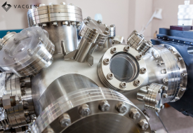
The vacuum environment in semiconductor manufacturing tools helps minimize impurities, control chemical reactions, and reduce the risk of contamination. This is critical for producing high-quality, defect-free semiconductor devices, as even tiny particles or chemical impurities can negatively impact semiconductor performance and yield. Therefore, many electromechanical components used in semiconductor manufacturing tools are carefully designed to be vacuum-compatible to meet these stringent requirements. VACGEN have a proven track record for machining and fabricating complex vacuum components supplied into the semiconductor industry. We can supply you with the critical instruments required to boost your business. Contact us today.