Introduction
Metrology plays a crucial role in the semiconductor industry by providing measurement and inspection solutions to ensure the quality, accuracy, and reliability of semiconductor devices. Various metrology equipment is utilised throughout the semiconductor manufacturing process, with many of the processes requiring a vacuum environment to perform affectively.
Vacuum environments help prevent contamination of sensitive semiconductor materials and devices. Contaminants in the air, such as dust particles or gases, can adversely affect measurements and compromise the quality of semiconductor components. A vacuum minimises the presence of these contaminants, ensuring the accuracy and reliability of metrology measurements.
Here are some common types of metrology equipment and their uses in the semiconductor industry:
Scanning Electron Microscope (SEM):
SEM is used for high-resolution imaging of semiconductor structures at the nanoscale. It provides detailed images of surfaces, helping in the inspection of features and defects.
Transmission Electron Microscope (TEM):
TEM is used to examine internal structures of semiconductor materials at an atomic level. It provides information on the crystallography, defects, and composition of materials.
In instruments like Scanning Electron Microscopes (SEMs) and Transmission Electron Microscopes (TEMs), a vacuum environment improves imaging resolution. The absence of air molecules reduces electron scattering, allowing for higher resolution imaging of semiconductor structures at the nanoscale. The vacuum environment also reduces the absorption of electrons by air molecules. This ensures that the electron beam interacts more effectively with the sample, leading to clearer and more detailed images.
Atomic Force Microscope (AFM):
AFM is used for high-resolution imaging of surfaces at the atomic level. It measures forces between a probe tip and the sample surface, enabling the creation of detailed topographic maps.
Ellipsometer:
Ellipsometers are used for measuring thin film thickness and optical properties. They help in controlling and optimising the deposition of thin films in semiconductor manufacturing. In thin film deposition processes, such as those monitored by ellipsometers, maintaining a vacuum environment helps control the deposition rate and uniformity of thin films. This is critical for ensuring the desired optical and electrical properties of semiconductor devices.
X-ray Diffraction (XRD):
XRD is used to analyse the crystal structure of semiconductor materials. It provides information on crystal orientation, strain, and composition, which is critical for optimising semiconductor device performance. Many semiconductor materials are sensitive to oxidation when exposed to air. A vacuum environment helps prevent the oxidation of surfaces, ensuring that the material properties remain stable during measurements. This is particularly important in techniques like X-ray Photoelectron Spectroscopy (XPS) and Auger Electron Spectroscopy (AES).
Focused Ion Beam (FIB):
FIB systems are used for milling, cutting, and imaging semiconductor samples at the nanoscale. They are valuable for sample preparation, cross-sectioning, and modification. Vacuum environments facilitate precise sample handling and manipulation in instruments like Focused Ion Beam (FIB) systems. The absence of air reduces friction and allows for more controlled movement of samples during milling, cutting, and imaging processes.
Metrology Microscopes:
Optical microscopes equipped with advanced imaging and measurement capabilities are used for inspecting semiconductor wafers, identifying defects, and measuring critical dimensions. Vacuum environments help reduce airborne vibrations, which can interfere with high-precision measurements. Instruments like interferometers and metrology microscopes benefit from a stable and vibration-free environment to achieve accurate results.
Laser Interferometer:
Laser interferometers are used for measuring distances with extremely high precision. In semiconductor manufacturing, they are employed for precise positioning and alignment of equipment. Vacuum environments help control temperature variations, minimising thermal effects on measurements. Maintaining a stable temperature is crucial in metrology to ensure the accuracy and repeatability of measurements, especially in instruments like ellipsometers and interferometers.
Wafer Inspection Systems:
Automated optical inspection (AOI) and electron beam inspection (EBI) systems are used for inspecting semiconductor wafers, detecting defects, and ensuring the quality of the devices. Semiconductor samples are often sensitive to environmental conditions. In a vacuum, the absence of air prevents oxidation and other reactions that could alter the properties of the sample. This is particularly important when inspecting delicate semiconductor structures at the nanoscale.
Summary
These metrology tools contribute to the overall quality and reliability of semiconductor devices by ensuring that manufacturing processes meet the stringent specifications required for modern electronic components. The precise measurements provided by these tools are essential for maintaining the performance and functionality of semiconductor devices in various applications. The use of a vacuum environment in metrology equipment within the semiconductor industry is essential for maintaining the cleanliness, stability, and precision required for accurate measurements and imaging at the microscopic and nanoscopic levels. It helps ensure the reliability and quality of semiconductor devices by minimising the impact of environmental factors on the manufacturing and measurement processes.
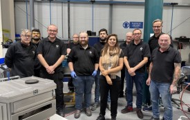
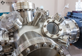
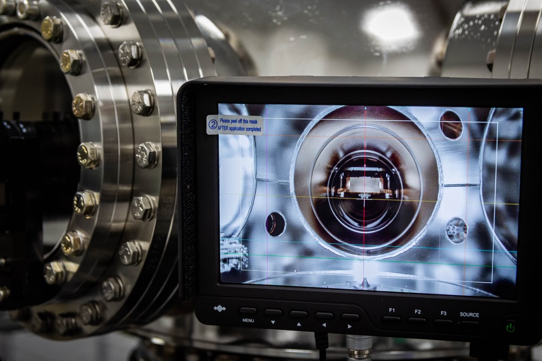
VACGEN have a proven track record for manufacturing precision technology utilised in wafer fabrication equipment including metrology and wafer inspection systems. For more information on how we can boost your business, get in contact today.