Introduction
The photomask is a critical part of the semiconductor fabrication process and inspection processes often involve sophisticated electromechanical assemblies to achieve high precision and reliability. Some of the key electromechanical assemblies commonly used in reticle inspection systems are XYZ stages, robotic arms, inspection and alignment equipment. In this blog we’ll take a look at various semiconductor inspection tools and their uses in the wafer inspection process.
Precision Stage Systems
Translation Stages: These stages provide precise movement in the X, Y, and sometimes Z directions to position the reticle accurately under the inspection optics.
Rotation Stages: Some reticle inspection systems include rotation stages to facilitate the examination of the reticle at different orientations.
Auto-Focus Systems
Z-Axis Actuators:These actuators are essential for maintaining focus during the inspection process. They automatically adjust the distance between the inspection optics and the reticle surface to accommodate variations in topography.
Reticle Handling Systems
Robotic Arms:Robotic arms are used for the handling and manipulation of reticles within the inspection system. They ensure safe and precise transportation of reticles between different stages of the inspection process.
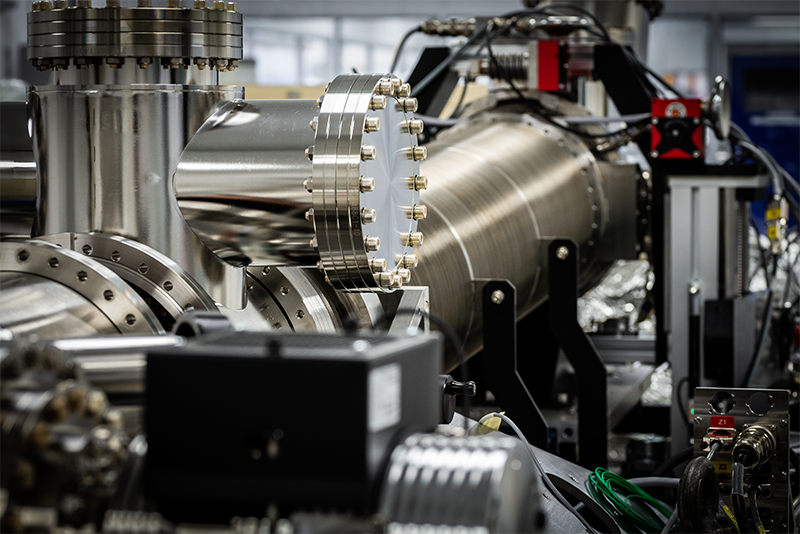
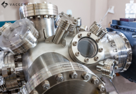
Load Ports: Load ports facilitate the loading and unloading of reticles from the inspection system, minimising the risk of contamination. These handling systems can be designed with ultra-high vacuum equipment at the core to provide you with a contamination free zone, a desirable quality in the semiconductor manufacturing process.
Pellicle Handling Mechanisms
Pellicle Frames and Holders:For reticles protected by pellicles, there are electromechanical assemblies designed to handle pellicle frames and holders. These assemblies ensure the proper positioning and removal of pellicles during inspection.
Illumination Systems
Light Sources: Electromechanical systems control the illumination sources used for inspecting the reticle. This may involve adjustable light intensity and wavelength selection to optimize defect detection.
Optical Inspection Modules
Objective Lenses: Precision electromechanical assemblies control the movement and positioning of high-resolution objective lenses over the reticle surface.
Beam Splitters and Mirrors: These components are manipulated to direct light to the reticle and capture reflected light for inspection.
Auto-Alignment Systems
Alignment Mechanisms: Electromechanical systems enable automatic alignment of the reticle with respect to the inspection optics. This is crucial for maintaining accuracy during the inspection process.
Vibration Isolation Systems
Isolation Tables: Precision reticle inspection requires a stable environment. Vibration isolation systems, often involving electromechanical components, are used to minimise external vibrations that could affect inspection accuracy.
Focus and Tilt Adjustment Systems
Electromechanical Tilt Stages:Some inspection systems include stages that allow controlled tilting of the reticle for angled inspections.
Focus Adjustment Mechanisms: Fine-tuning focus is critical, and electromechanical systems enable precise adjustments for optimal imaging.
Data Acquisition Systems
Position Encoders: These electromechanical components provide feedback on the position of various moving parts within the inspection system, contributing to closed-loop control and accurate positioning.
Temperature Control Systems
Thermal Management Components: Electromechanical systems are often used to control the temperature within the reticle inspection environment, ensuring stability and preventing thermal-induced distortions.
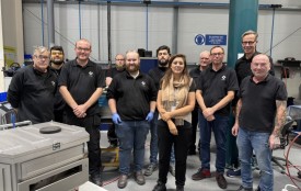
Some of the key components of these wafer or reticle inspection systems can be designed and manufactured at our UK headquarters. Our cleanroom facility and skilled work force are trained in Copy Exactly manufacturing methods to ensure our semiconductor customers can order with confidence.
Summary
These electromechanical assemblies collectively contribute to the high precision, automation, and reliability required for reticle inspection in semiconductor manufacturing. They play a crucial role in maintaining the quality and integrity of the photomasks used in the semiconductor lithography process. VACGEN specialise in custom manipulators designed for the semiconductor industry. Our capabilities include turning concepts into realisation with design and CAD support, acoustics and thermal dynamics experience and structural support when designing your semiconductor wafer processing equipment. Contact us today to start your journey.


