Introduction
The semiconductor industry relies heavily on vacuum technology for various processes and applications. Vacuum, in this context, refers to an environment with very low pressure and a near absence of gas molecules. Here are some key ways in which vacuum technology is used in the semiconductor industry:
Deposition Processes
Vacuum is essential for various deposition processes used in semiconductor manufacturing, such as chemical vapour deposition (CVD) and physical vapour deposition (PVD). These processes involve depositing thin layers of materials onto silicon wafers to create integrated circuits and other semiconductor components. A vacuum environment ensures precise control over the material deposition and reduces contamination from air molecules.
Etching
Vacuum is also employed in the etching processes used to remove specific areas of materials from semiconductor wafers. Dry etching methods, such as plasma etching, often use low-pressure environments to create highly anisotropic etching profiles, enabling the creation of intricate patterns and features.
Ion Implantation
Ion implantation is a critical step in semiconductor manufacturing, where ions of specific elements are embedded into the silicon wafer to modify its electrical properties. This process is carried out in a vacuum to ensure precise control over ion trajectories and implantation depths.
Wafer Handling and Transfer
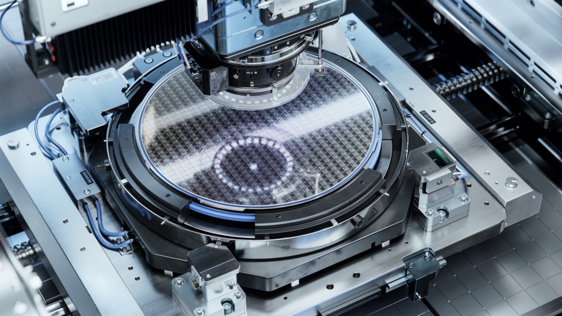
Vacuum technology is used for handling and transferring silicon wafers within the cleanroom environment to prevent contamination. Vacuum robotic arms and wafer handling tools are designed to transport wafers without contact, ensuring the utmost cleanliness.
Rapid Thermal Processing (RTP)
In RTP, semiconductor wafers are subjected to high temperatures in a controlled environment. Vacuum or low-pressure conditions can be used to prevent oxidation of the wafers at elevated temperatures, allowing for precise thermal treatments without introducing impurities.
Leak Testing
Vacuum technology is used to check the hermetic sealing of semiconductor packages and other components. Ensuring that no leaks are present is crucial for maintaining the integrity and reliability of semiconductor devices.
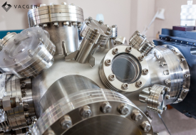
Vacuum Pumps
High-quality vacuum pumps are essential for maintaining the desired vacuum levels in various semiconductor manufacturing tools and chambers. These pumps can be categorised into different types, such as rotary vane pumps, dry pumps, and cryogenic pumps, depending on the specific requirements of the process.
Cleanroom Environments
Cleanrooms in the semiconductor industry are maintained under controlled atmospheric conditions, including low levels of airborne particles and contaminants. Maintaining a vacuum or controlled pressure within these cleanrooms helps to minimise impurities and maintain the cleanliness required for semiconductor fabrication.
In summary, vacuum technology plays a crucial role in the semiconductor industry, enabling precise and contamination-free processes for the production of microelectronic components. Vacuum-based processes are essential for achieving the high levels of precision and quality required in semiconductor manufacturing. VACGEN are a key supplier to various high-tech industries which require different levels of vacuum in their technology. All our vacuum components are assembled in a class 7 cleanroom facility with monitored airflow, helium leak checked and cleaned according to UHV standards to achieve precision in our vacuum technology. If you are looking for a vacuum component partner who understands the critical role of vacuum in your industry, then Contact VACGEN today.