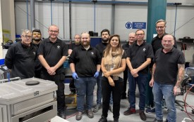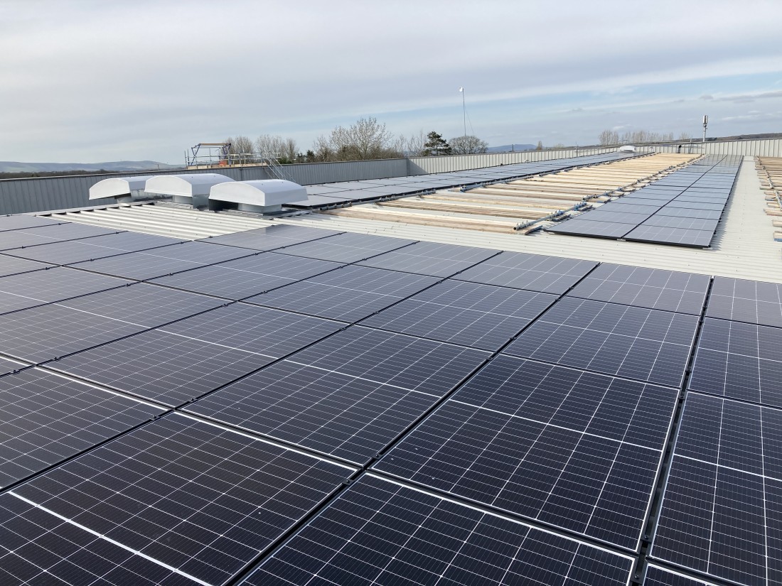
In case you haven’t heard already, VACGEN are going green. We’ve installed 609 solar panels on our UK headquarters roof and are soon to be installing EV charging points too.
To mark this occasion, we thought we’d take a look at the link between vacuum technology and solar panels, in particular the production of thin-film solar cells.
In the production of thin-film solar cells, vacuum technology plays a crucial role in various deposition processes used to create thin layers of semiconductor materials. Thin-film solar cells are distinct from traditional crystalline silicon solar cells as they use thin layers of semiconductor materials to absorb sunlight and convert it into electricity. The main thin-film technologies include amorphous silicon (a-Si), cadmium telluride (CdTe), copper indium gallium selenide (CIGS), and organic photovoltaic (OPV) cells.
Here's how vacuum technology is involved in the production of thin-film solar cells:
Deposition of Thin Layers:
Physical Vapor Deposition (PVD): PVD processes, such as evaporation and sputtering, are commonly used to deposit thin layers of semiconductor materials onto a substrate. In these processes, a vacuum environment is created to eliminate air and other contaminants that could interfere with the deposition. The substrate is placed in a vacuum chamber, and the semiconductor material is either evaporated or sputtered onto the substrate surface.
Chemical Vapor Deposition (CVD): CVD processes are used to deposit thin films by introducing precursor gases into a vacuum chamber. The precursor gases react on the substrate surface, forming a thin layer of the desired semiconductor material. CVD is often employed in the production of certain thin-film technologies, such as CIGS.
Annealing and Doping: After deposition, some thin-film solar cell technologies require annealing processes to improve the crystallinity and electrical properties of the deposited layers. Vacuum conditions are often maintained during annealing to prevent oxidation and ensure the desired material properties. Doping processes may also be carried out in a vacuum to introduce specific impurities into the thin-film layers, altering their electrical properties.
Encapsulation and Packaging: Once the thin-film layers are deposited and processed, the solar cell is often encapsulated to protect it from environmental factors. Vacuum technology may be involved in the encapsulation process to ensure that the encapsulant material adheres tightly to the solar cell and to remove any trapped air or moisture that could degrade performance over time.
Etching and Patterning: Vacuum-based processes, such as reactive ion etching (RIE) or plasma etching, may be used to selectively remove or pattern specific regions of the thin-film layers. This is important for creating the necessary structures and connections within the solar cell.
The use of vacuum technology in thin-film solar cell production helps create a controlled environment, minimising impurities and ensuring the uniformity and quality of the deposited layers. This contributes to the overall efficiency and performance of thin-film solar cells.
VACGEN's vacuum solutions support the development of sustainable technologies that address global energy challenges and environmental concerns. Whilst we are also working hard to minimise our carbon footprint by utilising green technologies throughout our manufacturing facility. Fingers crossed the sun starts to shine for our new solar panels and we can start harvesting those solar rays. If you require a bespoke vacuum technology solution, then contact us today.