Introduction
Material deposition refers to the process of adding or depositing material onto a substrate or surface. This can be achieved through various techniques and methods, each suited to different applications. For many of these applications, vacuum is an essential requirement to achieve the required quality.
Material deposition or thin-film deposition can be achieved through Plasma Vapour Deposition (PVD) Molecular Beam Epitaxy (MBE), Atomic Layer Deposition (ALD) and Chemical Vapour Deposition (CVD); and more. These variations in material deposition techniques allow for different profiles of material to be deposited onto a substrate or sample surface, building up complex material structures. Material Deposition is successfully utilised in applications such as microelectronics, material science and research, optics, coatings and semiconductor production; where the style of deposition required can depend on the nanoscale and complexity of the surface, chip or node which is being fabricated.
In this article we’ll look at some of the techniques used in material deposition and how these are utilised in advancing science and industry. We’ll also look at some real-life applications such as semiconductor wafer fabrication and why vacuum is a fundamental aspect in creating a successful environment for deposition.
The Different Styles of Material Deposition
Molecular Beam Epitaxy (MBE)
Molecular beam epitaxy is a deposition method commonly used for thin-film deposition of single crystals in semiconductor wafer fabrication. During the process, elements such as Gallium or Arsenic which are stored inside sources such as an effusion cell or electron-beam evaporator, are heated and directed towards an atomically clean substrate surface. The arriving constituent atoms form a crystalline layer in registry with the substrate, forming an epitaxial film. The process is repeated to build up layer upon layer to the desired thin-film structure, whilst being monitored by RHEED (reflection high-energy electron diffraction) equipment to observe growth in real-time. This precision application of molecules is particularly beneficial for the development of advanced semiconductor devices with specific electronic properties. An ultra-high vacuum environment of 1x10⁻¹⁰ mbar is typically required for the process of MBE, with routine bakeouts scheduled to consistently achieve these base pressures. UHV conditions are required to ensure minimal contamination and to allow precise control over the deposition process. The method is considered one of the fundamental tools utilised in the development of new nanotechnologies and is often used in R&D laboratories for semiconductor fabrication plants as well as in the fabrication processes as well as the fabrication of high-end semiconductor wafers.
Chemical Vapour Deposition (CVD)
Chemical Vapour Deposition (CVD) is a materials processing technique used for the deposition of thin films onto a substrate surface. In CVD, the chemical reactions take place at the surface of a substrate to produce a thin layer of material. Gaseous reactants, typically in the form of volatile precursor gases, are introduced into a reactor chamber, where they undergo chemical reactions to form a solid material. Substrates are placed within a vacuum chamber and often heated to a specific temperature to facilitate the chemical reaction and promote adhesion of the deposited material. Plasma-Enhanced CVD involves the use of plasma to enhance the chemical reactions and promote the deposition of thin films. This technique is widely used in various industries, including semiconductor manufacturing, optics and coatings. The control over film composition, thickness and uniformity in production of coatings for optical components, solar cells and various other applications is critical for specialised components to operate successfully. CVD allows for the deposition of thin films with excellent conformity to complex shapes and high aspect ratios.
Atomic Layer Deposition (ALD)
ALD is a thin film deposition technique used in various industries, particularly semiconductor manufacturing, electronics and material science. A highly controlled process that allows for the precise deposition of an atomic uniform layer of material onto a substrate surface. The vacuum chamber in which this happens, must be extremely clean and maintain a consistent level of high vacuum to prevent contamination. These specialised vacuum chambers offer precise control over temperature and gas flows. The equipment used for ALD is designed to facilitate the sequential exposure of precursors and ensure precise control over the deposition process. Atomic Layer Deposition is characterised by its layer-by-layer growth mechanism. It involves sequentially exposing the substrate to alternating precursors, typically in a gas phase. Each exposure results in the formation of a single atomic layer. Offering exceptional control over film thickness, this precision is crucial for applications in nanotechnology and semiconductor devices, where thin films with specific properties are required.
Physical Vapour Deposition (PVD)
PVD processes generally involve the vaporisation of a solid material (the target or source) and its subsequent condensation onto a substrate to form a thin film. This is typically done in a vacuum environment to minimise interference from gases and achieve better film quality. Unlike chemical processes, PVD methods involve the physical transfer of material from a source to a substrate. Two common PVD techniques include Sputtering and Evaporation: Sputtering: This method involves bombarding the target material with energetic ions (usually argon ions) to eject atoms or molecules, which then deposit onto the substrate. Evaporation: In this process, the target material is heated to a high temperature, causing it to evaporate and form a vapour. The vapour then condenses on the substrate to create the thin film. PVD allows for precise control over the properties of the deposited films, including thickness, composition, and microstructure. PVD coatings often exhibit high adhesion, hardness, and wear resistance. They can also enhance the corrosion resistance of materials. Common PVD coatings include metallic coatings (e.g., titanium nitride, chromium), decorative coatings (e.g., gold, silver), and functional coatings (e.g., anti-reflective coatings, barrier coatings). PVD is a versatile and widely used technology in manufacturing and research, offering control over film properties and enabling the deposition of thin films with specific characteristics tailored to different applications.
Pulsed Laser Deposition (PLD)
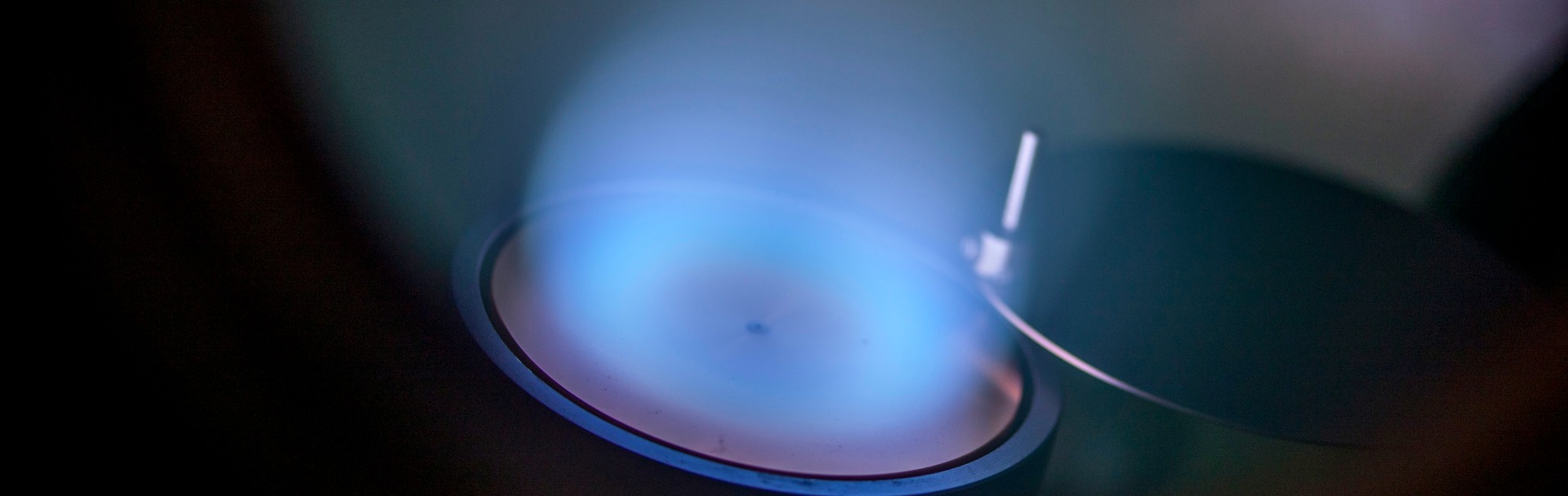
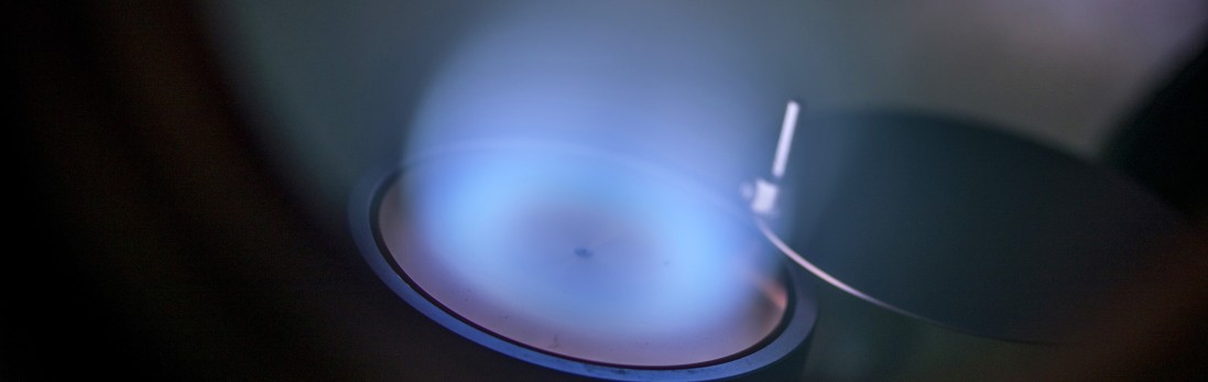
Pulsed Laser Deposition relies on laser ablation, where a high-intensity pulsed laser is focused onto a target material. This technique uses high power laser pulses (typically 108 Wcm-2) to melt, evaporate and ionise material from the surface of a target. This “ablation” event produces a transient, highly luminous plasma plume that expands rapidly away from the target surface and towards the substrate surface, depositing material onto a substrate surface. The laser-induced plume consists of atomic, ions and clusters of the target material. As the plasma plume makes contact with the substrate, the vaporised material condenses and forms a thin film on the substrates surface. The process allows for the deposition of various materials, including metals, oxides, nitrides, and complex compounds. While PLD has advantages in terms of precision and versatility, it also requires careful control of experimental parameters to achieve the desired film quality.
Why Vacuum is Necessary?
Vacuum conditions provide a stable and predictable environment for controlling the deposition rates. This is crucial for achieving uniform film thickness and desired properties. Some other factors include contamination prevention, improving adhesion and purity, reducing oxidisation rates and enhancing thin film properties.
Prevention of Contamination: In many deposition processes, maintaining a vacuum helps prevent contamination of the deposited material. Contaminants such as gases and particles in the air can affect the quality and properties of the deposited layer.
Controlled Environment: Vacuum environments allow for better control over the deposition process. Removing air and other gases helps in achieving a more uniform and controlled deposition of materials.
Improved Adhesion and Purity: Vacuum environments can enhance adhesion between the substrate and the deposited material. Additionally, a vacuum minimises the presence of impurities, leading to higher purity in the deposited layers.
Reduced Oxidation: Some materials are sensitive to oxidation, and a vacuum helps in reducing or eliminating the presence of oxygen, ensuring that the material deposited retains its desired properties.
Enhanced Film Properties: Vacuum conditions can influence the microstructure and properties of the deposited films, leading to improved mechanical, electrical, or optical characteristics.
Key Components of Each Vacuum System
Molecular Beam Epitaxy MBE
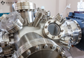
Due to the nature of MBE, the deposition chamber within the system, is often designed with an internal cryo-panel to optimise the vacuum pressure in the system. These cryo-panels require exemplary welding and skilled fabrication processes to achieve the perfectly formed double skinned vacuum chambers. Chambers for this application are also fitted with 316LN (1.4406) stainless steel flanges. This material is selected because of its hardness and durability to endure the multiple bakeout cycles without the risk of the knife edges softening and becoming defective. Other key components of the MBE system would include top flange assemblies for cryo-panel insertion and removal, effusion cells and deposition sources, all metal angle valves, linear and rotary drives for source shutters, substrate manipulators and load locks combined with transfer arms.
Chemical Vapour Deposition CVD
A vacuum environment helps ensure proper adhesion of the thin film to the substrate. Contaminants or moisture, trapped between the film and the substrate can negatively impact adhesion and film quality. Vacuum chambers are designed to withstand the varying temperature changes and chemical compositions which are introduced during these processes. By utilising the properties of stainless-steel instrumentation, we reduce the risk of vacuum leaks and introduction of rogue atmospheric elements.
Atomic Layer Deposition ALD
In an Atomic Layer Deposition (ALD) system, maintaining a controlled vacuum environment is crucial for the deposition process. Various vacuum instruments and components are required to achieve and maintain the necessary vacuum conditions. The vacuum chamber is the primary enclosure in which the ALD process takes place. It is designed to withstand vacuum conditions and equipped with multiple ports for the introduction of precursors, substrates and other necessary components. Pirani and Ion gauges are used to monitor and control the vacuum levels within the chamber. Whilst different types of valves, such as gate valves and right angles valves control the flow of gases and maintain specific conditions. A load lock system can be employed to introduce and remove substrates without breaking the vacuum in the main chamber. This helps to maintain a consistent vacuum environment during substrate handling.
Physical Vapour Deposition PVD
PVD systems consist of a vacuum chamber, a target source, a substrate holder, and various sources of energy (electric or thermal) to vaporise or sputter the target material. In a vacuum environment, there are fewer gas molecules that can interact with the evaporated or sputtered material. This reduces the risk of contamination of the thin film with unwanted elements from the atmosphere. Maintaining a vacuum allows for better control over the composition of the deposited film. If there were significant amounts of gases or impurities present, they could alter the film's properties and compromise its intended functionality.
Pulsed Laser Deposition PLD
Pulsed laser deposition often requires sample manipulation with continual rotation, to provide uniformity in the deposition process. Substrates are often aligned off centre to the target to ensure uniform layers to be deposited during the ablation of the material. VACGEN have various motorised designs for target and substrate manipulators with heating +900°C and cooling -150°C, whilst providing continual 360° rotation. Specialty viewports are also essential for PLD systems, these viewports must be able to withstand the laser frequency, allowing the beam to penetrate the viewport material to enter the vacuum chamber.
Summary
Material deposition is a versatile process with applications across various industries, and the use of vacuum is essential in many cases to control environmental factors and ensure the quality and performance of the deposited materials. VACGEN specialise in the design, engineering and manufacture of vacuum components including manipulation sub-assemblies, wafer fabrication equipment and vacuum chambers. Previous projects include cryo panels, complex vacuum chambers, effusion cells, evaporation and OLED sources, deposition manipulators with RF / DC bias, and more.
Choosing a supplier who understands the technology behind your system can be a daunting task, so we aim to support you through the design and engineering phase, all the way to completion of the finished article. If you are looking for a vacuum partner who performs to the highest standards, then contact us today for more information on how we can help you take the next leap forward.