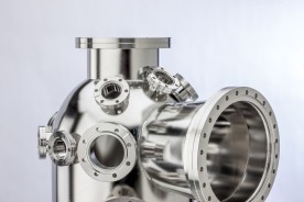
Material deposition refers to the process of adding or depositing material onto a substrate or surface. This can be achieved through various techniques and methods, each suited to different applications. For many of these applications, vacuum is an essential requirement to achieve the required quality.
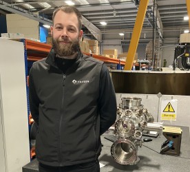
Recently VACGEN’s Sourcing Engineer, Seb, completed his first module as part of his Level 4 Chartered Institute of Procurement and Supply (CIPS) with a Merit. We caught up with Seb to learn more about why he decided to enrol for this qualification.
Today we’re celebrating Women and Girls in Science, Technology, Engineering and Mathematics Day. To mark the occasion we have interviewed our Monument Cell Leader - Carly.
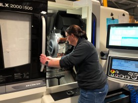
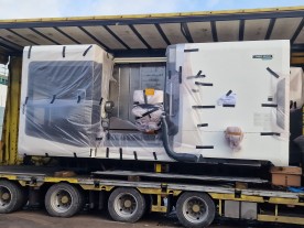
We are delighted to announce the acquisition of two advanced CNC machines from DMG Mori. These state-of-the-art machines represent a significant investment in our commitment to delivering unparalleled precision, repeatability, and efficiency in our production processes.
A Coordinate-Measuring Machine (CMM) is a device used in manufacturing and quality control to measure the physical geometrical characteristics of an object. It is commonly used in industries such as aerospace, automotive, and precision engineering. By using a coordinate measuring machine (CMM), VACGEN can guarantee precision, paramount in the modern and fast-changing manufacturing industry. Learn more about the CMM and they’re potential in the industry below.
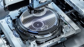
The photomask is a critical part of the semiconductor fabrication process and inspection processes often involve sophisticated electromechanical assemblies to achieve high precision and reliability. Some of the key electromechanical assemblies commonly used in reticle inspection systems are XYZ stages, robotic arms, inspection and alignment equipment. In this blog we’ll take a look at various semiconductor inspection tools and their uses in the wafer inspection process.
Metrology plays a crucial role in the semiconductor industry by providing measurement and inspection solutions to ensure the quality, accuracy, and reliability of semiconductor devices. Various metrology equipment is utilised throughout the semiconductor manufacturing process, with many of the processes requiring a vacuum environment to perform affectively.
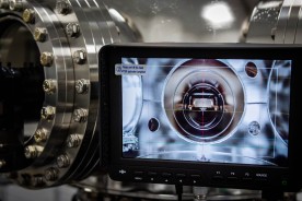
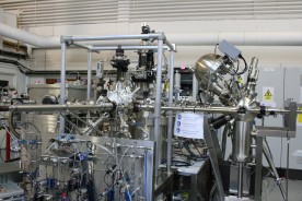
Photoemission spectroscopy is a powerful experimental technique used to study the elemental and electronic structure of materials in various states such as solids, liquids and gases. The application covers a wide range of scientific fields, with the main focus on surface chemistry and materials science. The most common forms of photoemission spectroscopy (PES) are X-ray photoelectron spectroscopy (XPS), Ultra-Violet photoelectron spectroscopy (UPS) and Angle Resolved photoelectron spectroscopy (ARPES). Let’s explore some of the fundamental aspects of this powerful tool.
A Nickel-Iron Alloy is a type of magnetic shielding material that is often used in electron spectroscopy chambers to minimise external magnetic interference. Electron spectroscopy techniques, such as X-ray photoelectron spectroscopy (XPS) or Auger electron spectroscopy (AES), are highly sensitive to magnetic fields. External magnetic fields can distort the trajectories of electrons, leading to inaccuracies in the measurements and affecting the overall performance of the spectroscopy system.
The semiconductor industry relies heavily on vacuum technology for various processes and applications. Vacuum, in this context, refers to an environment with very low pressure and a near absence of gas molecules. Here are some key ways in which vacuum technology is used in the semiconductor industry: